The common camera electronic device interfaces in the current market can be roughly classified into computer camera interfaces that are USB interfaces, smartphone camera interfaces that are MIPI interfaces, and some cameras (such as some hardware that supports DVP interfaces) that are DVP interfaces. Therefore, understanding the differences between these interfaces is basic knowledge that electronic engineers need to understand.
1.Interface name
USB is the abbreviation of Universal Serial Bus
MIPI is the abbreviation of Mobile Industry Processor Interface
DVP is the abbreviation of digital video port
CSI is the abbreviation of CMOS Sensor Interface

2.Introduction to the working principle of the camera
2.1. Working process
After the external light passes through the lens, it is filtered by the color filter and irradiated onto the sensor surface. The sensor converts the light transmitted from the lens into an electrical signal, and then converts it into a digital signal through the internal AD. If the sensor does not integrate DSP, it is transmitted to the baseband through DVP. At this time, the data format is RAW DATA. If DSP is integrated, RAW DATA data is processed by AWB, color matrix, lens shading, gamma, sharpness, AE and de-noise, and then output in YUV or RGB format. Finally, the CPU sends it to the framebuffer for display, and then you can see the scene captured by the camera.
2.2 Main components of Camera module
The camera is mainly composed of lens and sensor IC. Some sensor ICs integrate DSP, while others do not, but they also need external DSP processing.
Lens (lens) The lens structure of a general camera is composed of several lenses, which are divided into plastic lenses (Plastic) and glass lenses (Glass). The usual lens structures are: 1P, 2P, 1G1P, 1G3P, 2G2P, 4G, etc.
Sensor (image sensor) Senor is a semiconductor chip, there are two types: CCD (Charge Coupled Device) and CMOS (Complementary Metal-Oxide Semiconductor).
For CCD sensors, the charge signal is transmitted first, then amplified, and then A/D. The image quality has high sensitivity, good resolution, and low noise; the processing speed is slow; the cost is high and the process is complex.
For CMOS sensors, the charge signal is amplified first, then A/D, and then transmitted; the image quality has low sensitivity and obvious noise; the processing speed is fast; the cost is low and the process is simple.
The sensor converts the light transmitted from the lens into an electrical signal, and then converts it into a digital signal through the internal AD. Since each pixel of the sensor can only sense R light, B light, or G light, each pixel stores monochrome at this time, which we call RAW DATA data. To restore the RAW DATA data of each pixel to the three primary colors, ISP is required to process it.
ISP (Image Signal Processor) is mainly responsible for processing digital images and converting the raw data collected by the sensor into a format supported by the display. CAMIF (Camera Controller) is the camera interface circuit on the chip that controls the device, receives the data collected by the sensor and sends it to the CPU, and then sends it to the LCD for display.
3.Interface Introduction
3.1. [MIPI Interface]
MIPI cameras are commonly found in mobile phones and tablets, supporting high-definition resolutions of more than 5 million pixels. They are divided into MIPI DSI and MIPI CSI, corresponding to video display and video input standards respectively.
At present, MIPI cameras are widely used in embedded products such as driving recorders, law enforcement cameras, high-definition micro cameras, network surveillance cameras, etc.
MIPI (Mobile Industry Processor Interface) is an open standard and specification initiated by the MIPI Alliance for mobile application processors.

◆ MIPI Features
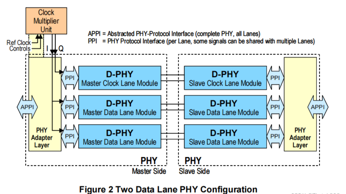
MIPI is a differential serial port transmission with fast speed and anti-interference. Mainstream mobile phone modules now use MIPI transmission, which uses 4 pairs of differential signals to transmit image data and a pair of differential clock signals;
It was originally designed to reduce the number of connections between the LCD screen and the main control chip, and later developed to high speed and support high-resolution display screens. Now it is basically a MIPI interface.
MIPI cameras have three power supplies: VDDIO (IO power), AVDD (analog power), DVDD (core digital power), and the power supply of cameras of different sensor modules is different
AVDD has 2.8V or 3.3V; DVDD generally uses 1.5V or higher, and the design of different manufacturers is different. 1.5V may be provided by the sensor module or externally supplied. If external power supply can be used, it is recommended to use external power supply, and the voltage must be greater than the internal DVDD; VDDIO voltage should be consistent with the level of MIPI signal line.
If the signal line is 2.8V level, VDDIO should also supply 2.8V. Some sensor modules may not supply VDDIO and provide it internally.
MIPI’s camera interface is called CSI, and MIPI’s display interface is called DSI.
3.2.[DVP interface]
The PCLK limit of the DVP bus is about 96M, and the trace length cannot be too long. All DVP maximum rates are best controlled below 72M, and the PCB layout is easier to draw.
The IPI bus rate LVDS interface is coupled, and the traces must be differentially equal in length and require protection, so the PCB traces and impedance control requirements are higher (generally speaking, the differential impedance requirement is between 85 ohms and 125 ohms).
DVP is a parallel port, requiring PCLK, VSYNC, HSYNC, D[0:11] – can be 8/10/12bit data, depending on whether the ISP or baseband supports it. MIPI is an LVDS low-voltage differential serial port, requiring only CLKP/N, DATAP/N – supports up to 4-lane, generally 2-lane can handle it. The MIPI interface has fewer signal lines than the DVP interface. Because it is a low-voltage differential signal, it generates less interference and has strong anti-interference ability.
The DVP interface is limited in signal integrity and rate. 500W can barely use DVP, and 800W and above use MIPI interface.
3.3. [CSI interface]
The CSI-2 interface specification is a camera serial interface released by the MIPI (Mobile Industry Processor Interface) Alliance in 2005.
As a new interface framework between camera devices and processors, it provides a flexible and high-speed device interface for portable, mobile phone cameras and other related industries [28]. Previously, traditional camera interfaces generally included data bus, clock bus, synchronization signal line control line, etc.

This camera physical interface occupies more data lines, and the logic design is also more complex. It requires strict synchronization including horizontal synchronization signal, vertical synchronization signal and clock signal, which puts higher requirements on both the camera and the receiver
In the process of high-speed transmission, directly using digital signals as data is easily interfered by other external signals, which is not as stable as differential signals. This also greatly limits its transmission rate and the maximum image quality that the camera can transmit in real time.
Based on the CSI-2 camera data transmission process, the data differential signal is used to transmit the pixel value in the video. At the same time, the CSI-2 transmission interface can be very flexibly simplified or expanded. For application scenarios with fewer interfaces, the CSI-2 interface can only use one set of differential data signal lines and one set of differential clock lines to complete the camera’s data serial transmission process, which reduces the load and can also meet a certain transmission rate. For large-array CCD cameras, the CSI-2 interface can also expand its differential data lines to meet the high-speed requirements of parallel transmission of multiple sets of data lines.
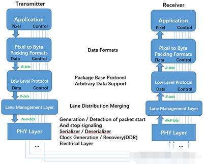
The CSI-2 interface also integrates the control interface CCI (Camera Control Interface), which is a full-duplex master-slave device communication control interface that supports a 400KHz transmission rate. It is compatible with the IIC standard interface of many existing processors, so it is very convenient to implement the control of the CCI Master Module on the Soc to the CCI Slave Module on the CSI-2 TX end. CSI physical protocol layer regulations CSI-2 software framework is mainly divided into three layers, namely application layer, protocol layer, and physical layer. The protocol layer can be further divided into pixel byte packaging layer/unpacking layer, LLP (Low Level Protocol) layer, and lane management layer. The main system software block diagram is shown below:

CSI protocol layer design:
Application layer: mainly designs the encoding and decoding format of the upper layer data stream, and specifies the mapping relationship between pixels and bytes;
Protocol layer: mainly includes pixel/byte packaging/byte unpacking layer, LLP layer provides synchronization mechanism for serial transmission data, and channel management layer provides data bit width expansion function, so as to flexibly adapt to different application scenarios;
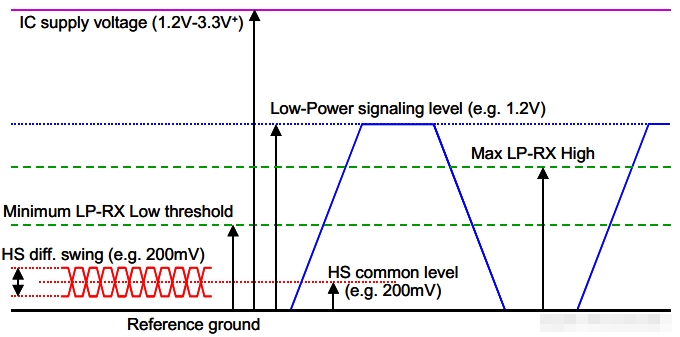
Physical layer: defines the basic transmission medium specification, determines the input and output characteristic parameters of the physical layer of the CSI-2 protocol, and determines its electrical characteristics and clock timing.


