This blog post comprehensively introduces the camera module CCM, working principle, 3A algorithm, camera module types and how to choose a manufacturer. Through this article, you can fully understand what a camera module is.
- What is a camera module?
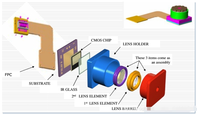
- The structure of a camera module
- The working principle of a camera module
- About the 3A algorithm of the camera module
- What are the common types of camera modules
- If you need a camera module, how do you choose a manufacturer?
1.What is a camera module?
Camera module, Camera Compact Module, abbreviated as CCM, is a module that integrates optical structure, sensor, interface and driver components. It can convert optical signals into digital signals to realize image acquisition and processing.
2.The structure of the camera module
Lens: Converges light onto the image sensor.
Voice coil motor (VCM): Completes the automatic focus of the camera.
IR-cut filter: Filters out invisible light to the human eye.
Image sensor: Converts optical signals into electrical signals.
Flexible printed circuit board (FPCB): connects the camera module to the main processor and transmits data.
The important components that determine the quality of a camera are:
Lens, image processing chip, sensor.
The key technologies of CCM are:
Optical design technology, aspherical mirror manufacturing technology, optical coating technology.

● Lens plays an important role in imaging, which is equivalent to the lens in the human eye. Using the refraction principle of the lens, the light of the scene passes through the lens to form a clear image on the focusing plane, and then the image is recorded through the photosensitive material CMOS or CCD, and converted into an electrical signal through the circuit. Lens generally consists of several lenses to form a lens structure. According to the material, it can be divided into plastic lens (plastic) or glass lens (glass). Glass lens is more expensive than resin lens. Plastic lens is actually a resin lens, and its optical indicators such as transmittance and photosensitivity are not as good as coated lens. The lens structures usually used by cameras are: 1P, 2P, 1G1P, 1G2P, 2G2P, 2G3P, 4G, 5G, etc. The more lenses, the higher the cost, and the better the imaging effect.

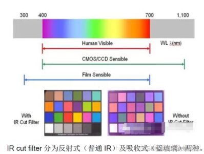
● IR filter is mainly used to filter out infrared light from the light entering the lens. This is because the human eye cannot see infrared light, but the sensor can sense infrared light, so the infrared light in the light needs to be filtered out so that the image is closer to the effect seen by the human eye.

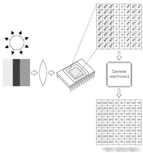
● Sensor is the core of the camera, responsible for converting the light signal passing through the lens into an electrical signal, and then converting it into a digital signal through the internal AD. Each pixel can only sense one of R, G, and B, so the data stored in each pixel is monochrome light, so the commonly mentioned 300,000 pixels or 1.3 million pixels means that there are 300,000 or 1.3 million photosites, and each photosite can only sense one kind of light. These most original photosites are called RAW Data (because each pixel of the sensor can only sense R light, B light, or G light, so each pixel stores monochrome at this time, which is called RAW DATA data).

Raw Data must be processed by ISP (Image Sensor Processor, a component of the Sensor module) to restore the three primary colors. That is to say, if a pixel is sensed as an R value, the ISP will calculate the G and B values of the R point based on the G and B values around the photosite, through interpolation and special effects processing, so that the RGB of the point can be restored.
There are currently two commonly used sensors, one is CCD (charge coupled device) components; the other is CMOS (metal oxide conductor) components.
■ CCD (Charge Coupled Device), charge coupled device sensor. Made of a highly sensitive semiconductor material, it can convert light into electric charge and convert it into electrical signals through an analog-to-digital converter chip. CCD consists of many independent photosensitive units, usually in megapixels. When the CCD surface is illuminated, each photosensitive unit will reflect the charge on the component, and the signals generated by all photosensitive units are added together to form a complete image.
■ CMOS (Complementary Metal-Oxide Semiconductor), complementary metal oxide semiconductor. Semiconductors mainly made of silicon and germanium are used to allow the coexistence of semiconductors with N(-) and P(+) levels on CMOS. The currents generated by these two complementary effects can be recorded by the processing chip and interpreted as images.
● Image processing chip DSP is an important part of CCM. Its function is to transfer the data obtained by the photosensitive chip to the central processor in a timely and fast manner and refresh the photosensitive chip. Therefore, the quality of the DSP chip directly affects the picture quality, such as color saturation, clarity, smoothness, etc. If DSP is integrated, the RAW Data will be processed by AWB (automatic white balance), color matrix, lens shading (lens shading correction), gamma (curve adjustment), sharpness, AE (automatic exposure) and de-noise, and finally output data in YUV or RGB format.
DSP structure framework:
ISP (Image Signal Processor), image signal processor or image signal processor
JPEG encoder, JPEG image encoder, divided into software and hardware.
ISP, Image Signal Processor, image signal processor; DSP, Data Signal Processor, digital signal processor.
ISP is generally used to process the output data of Image Sensor, such as AEC (Automatic Exposure Control), AGC (Automatic Gain Control), AWB (Automatic White Balance), Color Correction, Gamma Correction, Bad Pixel Removal, Auto Black Level, Auto White Level and other functions. DSP has more functions, it can do some photo taking and playback (JPEG encoding and decoding), video recording and playback (Video encoding and decoding), H.264 encoding and decoding, and many other aspects of processing, in short, it processes digital signals. ISP can be considered as a special type of DSP that processes image signals.
Note: What does ISP stand for, Image Signal Processor (Image Signal Processor) or Image Sensor Processor (Image Sensor Processor). Image Sensor Processor is equivalent to a part of the Sensor module, and DSP is the processor. Image Signal Processor is a real processor.
● DVP is divided into three parts: output bus; input bus; power bus;
● FPC flexible circuit board (flexible PCB), referred to as “soft board”, also known as “flexible circuit board”, plays the role of electrical signal transmission.
3.The working principle of the camera module
The light enters the camera through the lens, then passes through the IR filter to filter the infrared light, and finally reaches the sensor. The sensor can be divided into two types according to the material: CMOS and CCD. It can convert the optical signal into an electrical signal, and then convert it into a digital signal through the internal ADC circuit, and then transmit it to the DSP (if there is one, if not, the data is transmitted to the baseband chip baseband in the form of DVP, and the data format at this time is Raw Data, which will be processed later) for processing and conversion into RGB, YUV and other formats for output.
4.About the 3A algorithm of the camera module
AF Auto Focus
The purpose is to obtain a clearer image. There are two methods, one is the traditional focusing method, and the other is the image focusing method based on digital image processing. In the traditional method, automatic focusing is achieved by infrared or ultrasonic ranging. This type of focusing method is limited in some occasions. Therefore, in increasingly integrated, miniaturized and low-cost applications, the automatic focusing method based on digital image processing has more advantages. According to the lens imaging analysis, the optical transfer function of the lens can be approximated as a Gaussian function, which is equivalent to a low-pass filter. The greater the defocus, the lower the cutoff frequency of the optical transfer function. From the frequency domain, the increase in defocus will cause loss of high-frequency energy of the image, making the details of the image gradually blurred. From the spatial domain, the increase in defocus will cause the more dispersed the light intensity distribution function of the point light source imaging, the larger the resolvable imaging spacing, the overlap of adjacent pixels in the image, and the serious loss of image details. Therefore, the image clarity evaluation function is based on the high-frequency energy of the image edge. In digital processing methods, the key to automatic focusing is to construct the image clarity evaluation function. The image clarity evaluation function must have good unimodality and sharpness, and the calculation amount must be moderate, so that accurate focus can be achieved quickly.
AE automatic exposure
Exposure is a physical quantity used to calculate the size of the light flux from the scene to the camera. Only when the image sensor obtains the correct exposure can high-quality photos be obtained. Overexposure makes the image look too bright; underexposure makes the image look too dark. The size of the light flux reaching the sensor is mainly determined by two factors: the length of exposure time and the size of the aperture.
Automatic exposure using aperture mainly controls the aperture size according to the scene being photographed, so that the amount of light entering is maintained within a certain range. The cost of exposure control through aperture is relatively high. The mainstream technology used by low-end cameras in the market now realizes automatic exposure by adjusting the exposure time.
There are currently two automatic exposure control algorithm methods. One is to use the reference brightness value to evenly divide the image into many sub-images. The brightness of each sub-image is used to set the reference brightness value, which can be obtained by setting the shutter speed. Another method is to perform exposure control by studying the relationship between brightness and exposure value under different lighting conditions. Both methods have studied a large number of image examples and many different lighting conditions. And both require image databases collected under different lighting conditions. In practice, automatic exposure research needs to solve the following problems. The first is to determine whether the image needs automatic exposure. The second is how to adjust the digital signal after photoelectric conversion to find the automatic exposure capability compensation function during automatic exposure. Finally, it is to what extent the adjustment is most appropriate.
AWB automatic white balance
The basic principle of white balance is to restore white objects to white objects in any environment, that is, by finding the white block in the image and then adjusting the ratio of R/G/B, as follows:
R’= R * R_Gain
G’ = G * G_Gain
B’ = B * B_Gain
R’ = G’= B’
The AWB algorithm usually includes the following steps:
(1) Color temperature statistics: Count the color temperature according to the image statistics;
(2) Calculate channel gain: Calculate the gain of the R and B channels;
(3) Correct color cast: Calculate the correction of the color cast image according to the given gain.
5.What are the common types of camera modules
Classification by pixels:
Common pixel modules include 300,000 pixels (VGA), 1.3 million pixels (SXGA), 2 million pixels (UXGA), 3 million pixels (QXGA), etc. Modules with different pixels are suitable for different application scenarios. For example, low-pixel modules are suitable for occasions with low requirements for image quality, while high-pixel modules are suitable for occasions that require high-definition shooting.
Classification by focus method:
including FF (Fixed Focus) fixed-focus camera, MF (Micro Focus) two-speed zoom camera, AF (Auto Focus) auto-focus camera and ZOOM auto-focus camera. Fixed-focus camera is suitable for clear shooting within a certain depth of field, while zoom camera can change focal length and field of view as needed to achieve image zooming in and out.
Classification by interface type:
such as MIPI (Mobile Industry Processor Interface) interface
CSI (Camera Serial Interface) interface
DVP (Digital Video Port) interface
USB (Universal Serial Bus) interface
LVDS (Low Voltage Differential Signaling) interface
CVBS: Composite Video Broadcast Signal Interface
These interface types have their own characteristics and applicable scenarios in the field of camera modules. When choosing, you need to consider comprehensively according to specific needs and application scenarios.
6.If you need a camera module, how do you choose a manufacturer?
Camera modules are used to take photos and videos on a variety of mobile devices, such as smartphones, smart home appliances, industrial inspection, automotive electronics, medical endoscopes, and many other consumer and industrial applications.
In all application areas, cameras require high-level technology, high resolution, and low power consumption.
As a professional camera customization manufacturer, our R&D team will fully consider multiple factors such as application scenarios, performance indicators, optical performance, image processing, stability and durability, hardware design, software development, cost and supply, as well as compatibility and scalability, to provide satisfactory camera module professional models and strong support, from design to manufacturing, providing one-stop service, allowing you to focus on your professional field.
Customized solutions according to your camera module resolution requirements:
Customizable pixel requirements, such as 0.3MP-64MP, VGA/720P/960P/1080P/2K/4K.
For more information about OEM camera module related processes, please follow Gogoozx.


